概要
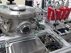
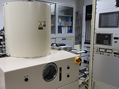
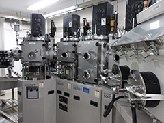
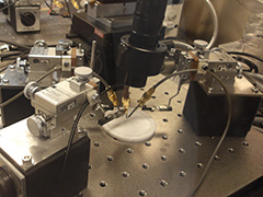
ここは,神戸大学大学院工学研究科電気電子工学専攻量子機能工学(EP3)北村・服部・張研究室のウェブページです。 当研究室では,薄膜材料を使った電子デバイスの開発とそれに関係する基礎研究を行っています。ここでいう薄膜とは,数10~数100 nm の厚さの膜を言います。 薄膜を使った応用としては電界効果トランジスタ,ガスセンサ,LED,太陽電池が考えられますが,当研究室が得意とするのは電界効果トランジスタです。 これまで,有機半導体や酸化物半導体の薄膜を使った電界効果トランジスタに関する研究での実績があります。 薄膜としては,半導体,金属,絶縁膜がありますが,当研究室ではこれらを製膜するための各種装置を有しています。 無機材料については,主にマグネトロンスパッタを使用しています。有機半導体については,専用の蒸着装置を所有しており,高品質の膜を製膜することができます。また,溶液プロセスとして,インクジェット法のほか,スピンコート法,ブレード法での製膜も可能です。 デバイス開発に関係して,薄膜の表面処理や表面への単分子膜の形成に関する技術を有しています。This is the web page of Kitamura-Hattori-Chang Laboratory, Department of Electrical and Electronic Engineering, Graduate School of Engineering, Kobe University. Our laboratory develops electronic devices using thin film materials and conducts basic research related to them. A thin film here means a film with a thickness of several tens to several hundred nm. Applications using thin films include field effect transistors, gas sensors, LEDs, and solar cells. We mainly focus on field effect transistors. we have developed high-performance field effect transistors using thin films of organic semiconductors and oxide semiconductors. Thin films include semiconductors, metals, and insulating films, and our laboratory has various equipment for forming these films. For inorganic materials, we mainly use magnetron sputtering. For organic semiconductors, we deposit the films using vapor deposition systme that produces high-quality films. As a solution process, we can deposit organic films by inkjet method, spin coating method, and the blade coating method. In relation to device development, we have technology related to surface treatment of thin films and the formation of monomolecular films on surfaces. In relation to device development, we have technique related to surface treatment of thin films and the formation of molecular layers on the surfaces.